Suzannah Povey-White, Author at Quorum Technologies Ltd - Page 2 of 3

T1_cpd_6nmPt1_0038_LMULX4s-1-1280x936.jpg

Plants are full of surprises, they are not only host for microorganisms but also for very small insects;

ImageJ=1.53f
unit=u00B5m

here we see a spider leg protruding from a cross-section of a banana leaf.

Specimen: Musa sikkimensis ( banana) leaf,  preparation and imaging from Anna Walkiewicz
Image: leaf cross-section with an unexpected inhabitant
Sample preparation: protocol for plant tissue preparation followed by Critical Point Drying (K850 CPD) and coating with 8nm of Pt (Q150V S plus).


Springtail-skin-1280x883.jpg

Springtails are extraordinary creatures, they are arthropods living in soil, plants and decaying material adapted to the environment by developing a special comb-like pattern on their skin. This rhombic-hexagonal structure is responsible for the non-wetting properties of the springtail body.

Sample: springtail colony from orchid bark. Sample preparation and imaging from Anna Walkieicz: bio preparation protocol followed by Critical Point Drying (K850 CPD) and coating with 8nm of Pt (Q150V S plus).


Picture1-1280x888.jpg

Pollen are small bioaerosol grains consisting of a single cell containing two male gametes essential for sexual reproduction of flowering plants. Typically, these bioaerosols range from 10 to 200 μm, are aerodynamic and low in density. These characteristics are essential for wind-pollination (anemophily) and/or insect-pollination (entomophily) – the transport of pollen from male stamen to the female stigma.

The grain wall is comprised of a tough chemically stable substance known as sporopollenin, which is highly resistant to environmental damage. It is punctuated with small openings called apertures which allows the male gametes to escape during pollination.

Pollen is typically classified by its 
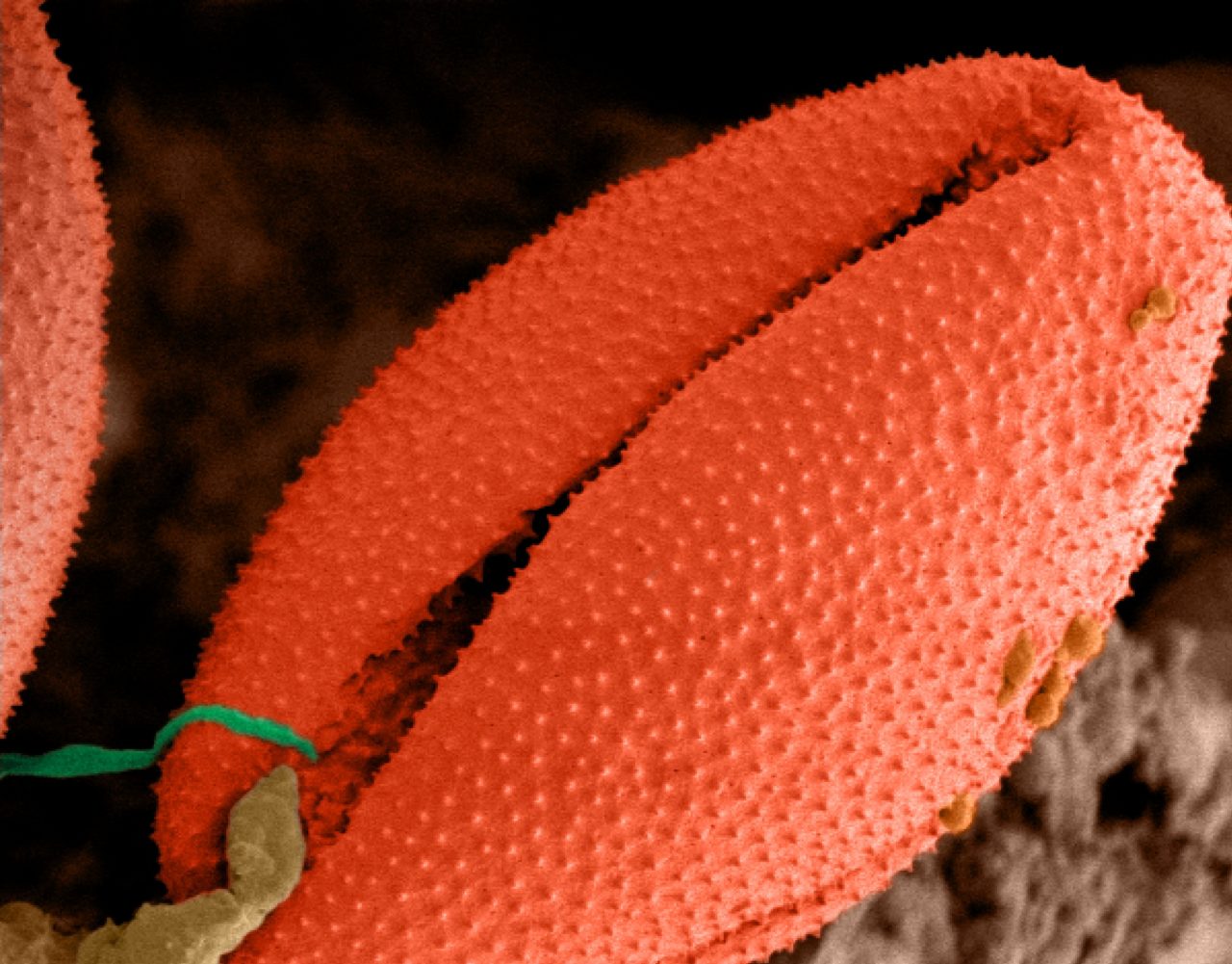
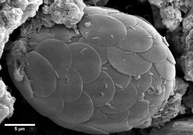
distinctive structural features, i.e., variation in size, shape, number of apertures and surface texture, which also makes it possible to identify and classify a plant at family and genus level, and often even species level.

Anemophilous (inconspicuous or non-flowering) plants typically produce enormous quantities of very lightweight pollen grains, usually with air-sacs. Whereas entomophilous (insect-loving) plants produce pollen that is relatively heavy, prickly, and sticky to cling to the insects attracted by the flowers’ nectar and showy colours.

SEM micrographs of pollen grains below are from a Papaver Nudicaule (Iceland Poppy) and a Geranium (Wild Purple Cranesbill) plant image imaged using a FE-SEM prepared using the Quorum PP3010 cryo-preparation stage by Dr Mark S. Taylor.


Picture2-1280x889.jpg

Calcium oxalate is frequently found in plants, leafy vegetable such as spinach, almonds and dates in the form of tiny needle like raphides. Whilst these play a central role in controlling calcium regulation, herbivory and metal detoxification, unfortunately if consumed, calcium oxalate can lead to kidney stones. Out of all the 3 forms of calcium oxalate, the monohydrate form is the one widely reported to cause kidney problems.

Images show needle like raphides of calcium oxalate crystals observed at Quorum Technologies using an Ultra high-resolution Field Emission Scanning Electron Microscope (FE-SEM), equipped with a PP3010 automated, column-mounted, gas-cooled cryo-preparation/ transfer stage chamber www.quorumtech.com

Small cross-sections of the plants were cut and mounted on a universal cryo-stub using mounting media – a 50:50 mixture of Tissue-Tek OCT (Optimal Cutting Temperature) compound (Agar Scientific) and colloidal graphite (G303 Sakura) to fix and aid electrical conductivity.

The Tissue-Tek OCT (Optimal Cutting Temperature) being a mixture of clear water-soluble polyethylene glycol with polyvinyl alcohol and the colloidal graphite a mixture of graphite, propan‑2‑ol, butanol and 1-methoxy-2-propanol. The cryo-stub with sample was then mounted onto a specimen shuttle plunge frozen (vitrified) in slushed nitrogen (LN2) and transferred under vacuum conditions to the cryo-preparation chamber.

On the preparation cold stage, maintained at -140°C (anti-contaminator -175°C), the vitrified samples were cleaved with a cold knife, sublimated at -90°C for 2 – 3 min and then coated in situ with Iridium using a current of 5 mA for 60 – 90 s to ensure electrical conduction. Cryo-SEM imaging at -140°C (anti-contaminator -175°C) was carried out at acceleration voltages 1-1.5 kV and emission currents 15 – 20 µA at working distances 8 – 12 mm detecting secondary emitted electrons.
(Imaged by Dr Mark Taylor of Quorum Technologies, UK) #microscopy #Cryoprep #quorumtech #samplepreparation


cpd_water-daphnias_algies6nmPt_0023_SEUL-2-2XX.jpg

Quorum Technologies would like to celebrate International #womeninscienceday,
Dr Anna E. Walkiewicz is the Applications Specialist at Quorum Technologies. She holds a PhD from the University of Birmingham, where she researched the recognition of chirality at the nanoscale.

ImageJ=1.53f
unit=u00B5m

This is shelled ameboid from fresh water sample.
Sample preparation: Biological sample prep protocol followed by critical point drying in Quorum K850 and coated with 6nm of Pt in Quorum Tech Q150V S Plus. quorumtech.com


Diatoms-combined2Small-1280x896.jpg

Imaging Spotlight. 

Diatom algae:
One of the most sophisticated frustule structures.
Sample preparation:
Biological tissue processing followed by critical point drying using Quorum Technologies K850 CPD and 8nm Pt coating in Q150VS Plus. Imaged by Dr Anna Walkiewicz, Applications Specialist
Daphnias algies


ImageForArticle_20774_16328329846236688.jpg

Electron microscopes use electrons rather than visible light to investigate and image samples, thus providing orders-of-magnitude enhancements on the magnification and resolution of traditional optical microscopes.

However, electron microscopes are much more complicated than optical microscopes, and the conditions that samples are subjected to are very difficult to work with.

SEM and TEM both depend on the transfer of electrons between a sample and the microscope itself, and thus imaging is performed under high vacuum. Moreover, samples must be conductive to enable electron transfer. This poses a difficulty for some sample types.

Although it is comparatively easy to use SEM or TEM to image solid metallic samples, for instance, imaging soft, hydrated and/or non-conductive samples — for example, biological tissues — can be challenging.

When left untreated, such samples lead to several issues. Moisture and gas from the sample easily evaporate inside the vacuum environment of an electron microscope sample chamber, thereby contaminating the microscope and damaging the sample.

Moreover, upon subjecting non-conductive samples to the incident electron beam within an electron microscope, the electrons do not conduct through the sample, making them accumulate in one place. This “charging” results in several imaging artifacts and can even make it impossible to image samples.

It is possible to solve these issues by the careful preparation of samples, specifically by sample coating. Using a layer of conductive material (carbon or metal) to coat samples has several purposes. There are two key reasons for coating: to make the sample conductive, which avoids “charging” effects, and to encapsulate samples to eliminate off-gassing or evaporation.1

Specifically, metallic coatings can facilitate better thermal conductivity, safeguarding the sample from heat damage from the incident electron beam. They can even localize the signal to the actual surface of the sample, thus enhancing the signal-to-noise ratio and secondary electron emission.

Carbon coatings offer certain distinct advantages. Carbon coatings for electron microscopy are amorphous, conductive layers transparent to electrons. This implies that carbon coatings are particularly valuable for making non-conductive samples amenable to energy-dispersive x-ray spectroscopy (EDS).2

Achieving High-Quality Carbon Coatings

For SEM and TEM applications, metallic coatings such as tungsten and gold can be done through sputtering. However, the same is not true of carbon. Although carbon can be sputter-coated, the resulting coatings exhibit high hydrogen concentrations, which makes carbon sputtering unsuitable for electron microscopy applications.

Alternatively, high-quality carbon coatings can be performed through thermal evaporation of carbon in vacuum. Two similar techniques can be used to achieve this — using carbon fiber or using a carbon rod.

In the carbon rod coating method, two carbon rods with a sharpened contact point between them are used. This is also called the Brandley method.

The process involves passing current between the two rods, ensuring very high current density at the sharpened contact point, which leads to very high levels of resistive heating. This causes the evaporation of carbon from the surface. This can be achieved with a ramped current or a pulsed current.

In the carbon fiber technique, a carbon fiber is mounted between two clamps, and a pulsed current is passed along it. This leads the carbon to evaporate from the surface of the fiber.

Both techniques exhibit unique differences in quality. The carbon fiber technique facilitates certain control over coating thickness by tweaking the number of current pulses and a pulse length. This makes it appropriate for TEM grid applications and analytical SEM applications like EDS and electron backscatter diffraction (EBSD). Yet, pulsed carbon fiber coatings essentially contain higher levels of debris.

Carbon rod coatings are “cleaner” and of better quality. Carbon rod coatings made in high vacuum with ramped current offer the maximum quality coatings, suitable for high-resolution TEM applications and crucial SEM applications.

In its pulsed version, the technique can be employed to achieve thicker coatings for SEM, particularly for wavelength-dispersive X-ray spectroscopy (WDS) and EBSD. In such applications, it is important to select carbon rods with the maximum purity to achieve the maximum possible coating quality.

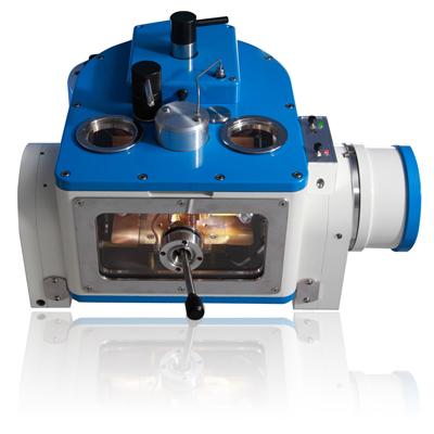
Carbon Coating Solutions from Quorum Technologies

Quorum Technologies has come up with the new Q Plus Series that offers an all-in-one solution to attain high-quality carbon coatings for all electron microscopy applications.

With the ability to coat both carbon fiber/cord and carbon rod, the carbon evaporators employ easy-change inserts to allow users to easily switch between the two modes.

The new Q150V Plus from Quorum Technologies offers the highest vacuum of 1 x 10⁻⁶ bar for superior results. The lower background pressure implies oxygen, nitrogen and water vapor are eliminated from the coating chamber, restricting chemical reactions while executing the coating process. This leads to impurities or defects. Lower scattering also implies amorphous carbon films of higher purity and high density.

References

  1. Goldstein, J. I. et al. Coating Techniques for SEM and Microanalysis. in Scanning Electron Microscopy and X-Ray Microanalysis: A Text for Biologist, Materials Scientist, and Geologists (eds. Goldstein, J. I. et al.) 461–494 (Springer US, 1981). doi:10.1007/978-1-4613-3273-2_10.
  2. Heu, R., Shahbazmohamadi, S., Yorston, J. & Capeder, P. Target Material Selection for Sputter Coating of SEM Samples. Microscopy Today 27, 32–36 (2019).
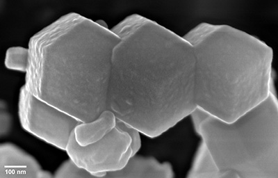
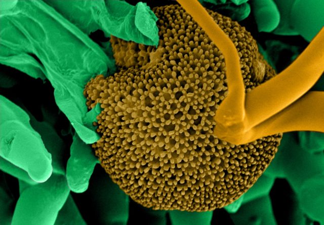
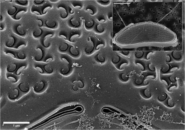
  3. Image shown – Fungi spores on a TEM grid (Cu, 300 mesh with 5nm carbon film produced with Q150VES Plus coater). Image Credit: Quorum Technologies

crystals_2nmAuPd_V_0058_mag100k.jpg

Electron microscopy techniques rely on the transfer of electrons between sample and microscope. For conductive samples, this is easily achieved – however, non-conductive, or poorly conducting samples must be coated with an electrically conductive coating to produce usable images. A high-quality coating is essential to obtain high-quality images. Quorum Technologies developed the Q Plus Series to provide researchers with a versatile and high-performance coating to rival major manufacturers, without the associated price tag.  

The Role of Coatings in Electron Microscopy

Scanning Electron Microscopes (SEM) and Transmission Electron Microscopes (TEM) work similarly to Optical Microscopes but rather than probing materials using light, they use electrons. Optical microscopes are diffraction-limited (to a maximum resolution of about 200 nm) whereas electron microscopes can produce beams of electrons with much smaller wavelenght1 and surpass the resolving power of optical microscopes by several orders of magnitude. As a result, they are the most powerful microscopy techniques in the world.

Using electrons instead of light, however, introduces other complications. Both techniques (SEM and TEM) rely on the transfer of electrons between sample and microscope; therefore, it can be difficult (or near impossible) to obtain a usable image signal from samples with poor or no conductivity. This is especially true of SEM, where samples are bombarded with an electron beam: poorly conductive or non-conductive samples will rapidly accumulate charge under these conditions, leading to image distortion as well as thermal and radiation damage to the sample. In extreme cases, the sample may accumulate sufficient charge to decelerate the primary beam, acting as an “electron mirror” and preventing an image altogether.2

To overcome this, poorly conducting samples are coated with a thin layer of metal or carbon. This makes the surface conductive, eliminating charge accumulation and enabling a better signal to be obtained by the microscope. Coating techniques are widely used for imaging biological or organic samples since these are typically non-conductive and easily damaged by the electron beam.

While the primary role of coating in SEM is to increase electrical conductivity and prevent “charging”, it also has several other useful effects:

  • Coating a sample with a thermally conductive material such as gold, silver, copper, aluminium can reduce thermal damage from the primary electron beam.
  • Particulate matter and fragile organic samples can be mechanically stabilized and held in place by a thin layer of carbon.
  • Coating organic samples that contain trapped gas or moisture protects both sample and microscope from being contaminated by off-gassing.
  • Metallic coatings can be used to minimize the volume of penetration of the electron beam, localizing scanning to the very surface of a sample. This can also dramatically increase the emission of secondary and backscattered electrons.

Download our Guide to Coating for Electron Microscopy Here


The Impact of Coating Quality

When working with a coated sample in an electron microscope, it is the coating itself that gets directly imaged. The quality of the coating, therefore, places a hard limit on the quality of the images that can be obtained.

When imaging very small structures (such as electrospinning fibres doped with copper nanocrystals), depositing a coating that is too thick can easily bury meaningful information. It is vital that coating thickness can be precisely controlled and tailored to the features that are being interrogated.3

In the worst cases, poor quality coating equipment introduces contamination and can irreparably damage samples. Researchers often opt for cheap coaters to save money, only to find that their costs increase due to additional microscope time and ruined samples.

However, thanks to the Q Plus Series from Quorum Technologies, it is no longer necessary to pay a premium to obtain state-of-the-art coatings.

The Q Plus Series: Affordable and High-Quality Coating

The Q Plus Series is the latest iteration of Quorum’s world-leading range of coaters; offering cutting-edge sputter and evaporation coating in a single easy-to-use platform. Quorum’s turbomolecular-pumped coaters are suitable for both oxidizing and non-oxidizing metals, while our low-cost rotary-pumped sputter coaters are suitable for non-oxidizing metals. The Q Plus Series is suitable for sputter coating and evaporating carbon coating for SEM, FE-SEM and TEM applications.

This new range of coaters is designed to enable researchers to exercise precise control over coating thickness, whatever their application requirements. For the highest level of performance, the Q150V Plus provides an ultimate vacuum of 10-6 mbar; removing oxygen, nitrogen and water vapour from the chamber and eliminating chemical reactions during the sputtering process. The Q150V Plus also enables the production of finer grain size and thinner coating for ultra-high-resolution applications (beyond 200,000x magnification). Low scattering enables the formation of high-purity amorphous carbon films of high density.

All models in the Q Plus Series feature a touch-screen interface as well as status LEDs and audio notifications for straightforward and intuitive control. Integrated 16 GB memory allows the storage of over 1000 recipes to be stored, and a USB port enables upgrades and downloads of log files.

To find out more about the Q Plus Series of coaters, view our brochure or get in touch with us today.

To view our latest webinars on coating technologies, we invite you to view our series here:
  1. Practical advice in sample preparation for SEM
  2. How to achieve appropriate metal coating quality for my application
  3. Carbon coatings and Glow Discharge for TEM


References and Further Reading

  1. The Diffraction Barrier in Optical Microscopy. Nikon’s MicroscopyU https://www.microscopyu.com/techniques/super-resolution/the-diffraction-barrier-in-optical-microscopy.
  2. Goldstein, J. I. et al. Coating Techniques for SEM and Microanalysis. in Scanning Electron Microscopy and X-Ray Microanalysis: A Text for Biologist, Materials Scientist, and Geologists (eds. Goldstein, J. I. et al.) 461–494 (Springer US, 1981). doi:10.1007/978-1-4613-3273-2_10.
  3. Ahire, J. J., Neveling, D. P. & Dicks, L. M. T. Polyacrylonitrile (PAN) nanofibres spun with copper nanoparticles: an anti-Escherichia coli membrane for water treatment. Appl Microbiol Biotechnol 102, 7171–7181 (2018).


pp3000T.jpg

Quorum’s PP3000T has now reached end-of-life support.

Please be aware if you have one still installed you will no longer be able to receive parts or service support from Quorum Technologies Ltd.

If you have any queries, please don’t hesitate to contact the sales team at [email protected]

All products currently available, in support, or no longer supported can be found on our website

https://www.quorumtech.com/products-and-parts-supported/


UNITED KINGDOM

Headquarters

Judges House, Lewes Road,
Laughton, East Sussex.
BN8 6BN

+44 1323 810981

www.quorumtech.com

[email protected]

UNITED KINGDOM

Working Hours

8.30 – 5.00 pm Mon – Thu
8.30 – 4.00 pm Fri
QUICK LOOK

Latest News


No more posts


GET IN TOUCH

Follow Our Socials

Keeping in contact with our customers via social platforms as well as traditional telephone and email.